
Intro
Since quite some time now, I’ve been intrigued by the Zilog eZ80 which is a successor of the well known Z80. While the eZ80 remains binary compatible with the Z80 it does have some interesting extensions like a flat 24 bits address space (no ugly 64k segments!) allowing to address up to 16 MByte. More info can be found on this Wikipedia page.
If you search a bit, then you can quite a few hobby projects using the eZ80. For me, the most interesting design was the Z20X open source computing system by Konstantin Dimitrov. This design was also featured on Hackaday. When PCB’s became available on Tindie as well, I had no excuse anymore for not starting a eZ80 project (well I was still busy with my 6845 based terminal of course but shiny new project …).

What do we need
Hardware
Next to the PCB(s) and it’s components, we need something to program the eZ80. The Z20X PCB already contains a connector for the ZDI (Zilog Debug Interface) interface. So we need something that allows us to connect our development PC with that ZDI connector. Zilog provides their USB Smart Cable for this. The link goes to Mouser but you can find/buy this in a lot of places. The manual for this cable can be found e.g. here.
Software
To write/compile/upload code for the eZ80, we need the ZDS II (Zilog Development Studio). Luckily for us, this is a free download and doesn’t even need an account. ZDS II v5.3.4 seems to be the latest version.
While you’re downloading, you’d best download all the (relevant) documentation from there as well. Click on eZ80 to see all the documentation.
Setting up a simple ‘Hello World’ project
Now that we have everything that’s needed (I’ll not go into how to install ZDS II and the driver for the USB Smart Cable), let’s start with our first project.
Since the Z20X doesn’t have a LED to build a BlinkenLight project we will have to be a bit more ambitious and build a Hello World project using a serial port (UART0 in our case).
Create a z20x-HelloWorld folder somewhere convenient on your
development PC.

Start up the ZDS II and under the File menu, select New Project. We see the kind of dialog box as shown below. For File name, we now specify the name of our project. I choose z20x-HelloWorld for this project. This will create a z20x-HelloWorld.zdsproj file in the z20x-HelloWorld folder.

Clicking on Select brings us to the next dialog where, for this simple project, we only need to change the CPU to the eZ80F92 as used in the Z20X:

Clicking on the Continue button brings us to the Step 1 - Build options dialog box as shown below. Nothing needs to be changed here and we can immediately press the Next button.

We arrive now in the Step 2 - Target and Debug Tool Selection dialog box as shown below and now it becomes a bit more complex.
The first thing to do is setting the Debug Tool. Make sure this is set to USBSmartCable.
The Use Page Erase Before Flashing check box at the top of the dialog can be left checked. When checked, the internal Flash memory of the eZ80 will be page erased. When unchecked, the internal Flash is configured to be mass-erased when the code is downloaded.
We also see 4 targets which you should consider as a template to start your own project from. From the list of templates, I select the generic eZ80F92_99C0873_Flash target to start from. Then I hit the Copy button to create my own copy of this generic template.

Once we hit the Copy button we’re presented the dialog as shown below. We only need to specify the name we wish to give the new target which will be a copy of the eZ80F92_99C0873_Flash target. In this case, I choose the name eZ80F92_Flash.

Hitting the OK button brings us back to the previous dialog box. We now see 5 targets (instead of 4 previously) because our new eZ80F92_Flash target has been added to the list.
Select the eZ80F92_Flash target and check its check box as well to indicate we want to use this target.

We’re not done yet with this dialog box. We now need to set up the target as well. For this, hit the Setup button (while making sure the eZ80F92_Flash target is selected) and we’re presented with a new dialog box as shown below.
Here we need to make quite a few modifications. The dialog box has 6 sub boxes. I’ll go everyone but not in a clock wise order:
- External RAM:
- Here we can specify where the external RAM range. I did
choose a range from
0x400000to0x47FFFFfor the 0.5 MByte external RAM chip on the Z20X. - This external RAM range specifies a range of RAM available to use as “scratch-pad” memory by ZDS for internal Flash memory page erase. The contents of the external RAM range is first saved and then restored again after a Flash erase operation.
- Note: If external RAM is not available, the external RAM range must be set to the internal RAM address range of the eZ80.
- Here we can specify where the external RAM range. I did
choose a range from
- External Memory/IO:
- For this simple example, we only need to configure the external RAM chip which is selected by CS0 in the Z20X computer.
- We specify its lower and upper bounds as
0x400000and0x47FFFF. - Control Register:
- This register controls the wait states for the memory
region when the selected chip select is active. This
determined by bits [7:5]:
- 000 0 WAIT states are asserted when this Chip Select is active.
- 001 1 WAIT state is asserted when this Chip Select is active.
- 010 2 WAIT states are asserted when this Chip Select is active.
- 011 3 WAIT states are asserted when this Chip Select is active.
- 100 4 WAIT states are asserted when this Chip Select is active.
- 101 5 WAIT states are asserted when this Chip Select is active.
- 110 6 WAIT states are asserted when this Chip Select is active.
- 111 7 WAIT states are asserted when this Chip Select is active.
- Bit 4 determines if the chip select is configured as a
memory select or as a I/O select:
- 0 Chip Select is configured as a Memory Chip Select.
- 1 Chip Select is configured as an I/O Chip Select.
- Bit 3 enables/disables the chip select:
- 0 Chip Select is disabled.
- 1 Chip Select is enabled.
- Bits [2:0] are reserved for future use.
- We want to enable the Chip Select and use 0 Wait States
for our external memory which gives us the hex value
08.
- This register controls the wait states for the memory
region when the selected chip select is active. This
determined by bits [7:5]:
- Bus Mode:
- Bits [7:6] BUS_MODE
- 00 eZ80® bus mode.
- 01 Z80 bus mode.
- 10 IntelTM bus mode.
- 11 Motorola bus mode.
- Bit 5 AD_MUX
- 0 Separate address and data.
- 1 Multiplexed address and data appears on data bus DATA[7:0].
- Bit 4
- Reserved.
- Bits [3:0] BUS_CYCLE
- 0000 Not valid.
- 0001 Each bus mode state is 1 CPU clock cycle in duration.
- 0010 Each bus mode state is 2 CPU clock cycles in duration.
- 0011 Each bus mode state is 3 CPU clock cycles in duration.
- 0100 Each bus mode state is 4 CPU clock cycles in duration.
- 0101 Each bus mode state is 5 CPU clock cycles in duration.
- 0110 Each bus mode state is 6 CPU clock cycles in duration.
- 0111 Each bus mode state is 7 CPU clock cycles in duration.
- 1000 Each bus mode state is 8 CPU clock cycles in duration.
- 1001 Each bus mode state is 9 CPU clock cycles in duration.
- 1010 Each bus mode state is 10 CPU clock cycles in duration.
- 1011 Each bus mode state is 11 CPU clock cycles in duration.
- 1100 Each bus mode state is 12 CPU clock cycles in duration.
- 1101 Each bus mode state is 13 CPU clock cycles in duration.
- 1110 Each bus mode state is 14 CPU clock cycles in duration.
- 1111 Each bus mode state is 15 CPU clock cycles in duration.
- I choose the eZ80 bus mode and Each bus mode state is 1 CPU
clock cycle in duration. Combined this gives us a
0x01hex value for the Bus Mode register.
- Bits [7:6] BUS_MODE
- PC/STACK Registers:
- For the Program Counter we use
0since we will position the internal Flash Memory starting from address0x000000. - For the SPL Stack Pointer (which is the stack pointer
when we run in 24 bit ADL mode) we choose
0x480000, which is at the end of the external RAM region. - For the SPS Stack Pointer (which is the stack pointer when we run in 16 bit Z80 mode), we can keep the default 0xFFFF value.
- For the Program Counter we use
- Internal Memory:
- The eZ80F92 has both 8K Static RAM and 128K Flash on board. Here we can specify where they will be located in its memory map.
- Internal RAM: We keep the internal RAM enabled and we set
the Address Upper Byte to B7 (meaning it will start from
address
0xB70000). - Flash: Also here we enable the Flash and we set its
Address Upper Byte to 00 (meaning it will start from
address
0x000000).- We can also set the number of Wait States when accessing the internal Flash. When a new project is created, ZDS II will suggest the optimal number of wait states for you assuming you filled in the clock frequency corrected. This can be seen by an ***** appended after the Wait State value in the Drop Down List.
- The wait states value is based on the value of the system clock frequency according to the following table:
Wait States - System Clock (MHz)0 ............. <12 MHz1 ............. 12–23.9 MHz2 ............. 24–35.9 MHz3 ............. 36–47.9 MHz4 ............. 48–59.9 MHz5 ............. 60–71.9 MHz6 ............. 72–84 MHz7 ............. >84* MHz- 5, 6, and 7 wait states are not recommended for performance reasons.
- Clock:
- Here we can specify the frequency of the crystal that is present on the Z20X board. This is important for baud rate calculations. Our example code will calculate the correct value for the baud rate generator register (brg) based on the value we fill in here. I use a 18.432 MHz crystal on my board (instead of the specified 18 MHz in the BOM). See later as well.
- Mode:
- Here we specify if the eZ80 in this project starts up in 24 bit ADL mode or in Z80 16 bits addressing mode. We can leave this boxed checked for this simple project.
- Note: This information is used only by the Debugger and does not affect your code initialization. The actual mode needs to be in your source files.

We’re not done yet with the above dialog box. We need to further configure the Flash by clicking on the Configure Flash button. We’re then presented with the dialog box as shown below.
- Internal Flash: Make sure the check box is checked.
- External Flash: Make sure the check box is unchecked.

Now we can finally click twice on the OK button (once for the Target Flash Settings dialog and once for the parent Configure Target dialog). And we get back to the Step 2 - Target and Debug Tool Selection and there we can now finally hit the Next button to bring us to the Step 3 - Target Memory Configuration dialog as shown below.
Here we specify the Linker Address Spaces and the Link Configuration:
- Linker Address Spaces:
- ROM: Set this to
0x000000-0x01FFFF(corresponds to the location and size of 128K of the internal Flash). - RAM: Set this to
0x400000-0x47FFFF(the same values as we had to enter earlier to define the external RAM).
- ROM: Set this to
- Link Configuration:
- We can keep this to Standard for this simple project.

And we can finally press the Finish button now and the IDE will present itself.
But we’re still not done yet… We still need to make small changes to the project settings. For this, go to the Project menu and select Settings.

We’re now presented the dialog below (showing the ZSL pane - after clicking on the ZSL on the left).
Our Hello World project will use UART0 which is Port D of the eZ80 GPIO ports. So, in the Ports box, we check Port D and in the Uarts box, we check UART0:

Now we’re finally done with setting up the project and we can start adding some code!
And this is the code for this project:
/*****************************************************************************
 *  This program will exercise the eZ80Acclaim! UART.  The UART will be used
 *  to print a few messages and echo any character it receives from the
 *  Console port.  The target specific information is as follows:
 *
 *  Target
 *  ==========================================================================
 *    eZ80F91
 *    ----------------------------------------------
 *      Select Ethernet/Serial/USB in Settings->Debugger from Project menu.
 *      The program output will be sent to UART0.
 *
 *      UART Parameters (default):
 *        57600 bps, 8 bits per character, No parity, 1 stop bit, No flow ctrl
 *
 *    Simulator
 *    ----------------------------------------------
 *      Select Simulator in Settings->Debugger from Project menu. The program
 *      output will be displayed in the Debug tab on the output window.
 *
 *  Project Settings and Build Configurations
 *  ==========================================================================
 *    Debug
 *    ----------------------------------------------
 *      The settings in this configuration allow the program to run on
 *      the Simulator and on the development platform in RAM during a
 *      debug session.
 *
 *    Release
 *    ----------------------------------------------
 *      The settings in this configuration allow the program to reside
 *      and execute from internal Flash in the eZ80F91 on the mini module.
 *
 *  Example Output
 *  ==========================================================================
 *    ZiLOG Developers Studio
 *    i = 5
 *    d = 25
 *    f = 1.260000
 *    eZ80F91 5 25 1.260000
 *
 *   Change History:
 *   12/02/11 - Fixed UART when ZSL is selected
 *
 ****************************************************************************/
#include <eZ80.h>
#include <stdio.h>

#define UART                 0			// change to 1 when using UART 1
#define UART_BPS             57600
#define UART_DATA_BITS       8
#define UART_PARITY          0
#define UART_STOP_BITS       1

#ifdef _EZ80190
#define DEVICE_NAME          "eZ80190"
#define UZI_MODE_UART        (unsigned char)0x01
#endif

#ifdef _EZ80L92
#define DEVICE_NAME          "eZ80L92"
#endif

#ifdef _EZ80F93
#define DEVICE_NAME          "eZ80F93"
#endif

#ifdef _EZ80F92
#define DEVICE_NAME          "eZ80F92"
#endif

#ifdef _EZ80F91
#define DEVICE_NAME          "eZ80F91"
#endif

#if !defined(_ZSL_UART_USED)
#if (UART==1)
#define	UART_FCTL	     	 UART1_FCTL
#define UART_RBR             UART1_RBR
#define UART_THR             UART1_THR
#define UART_BRG_L           UART1_BRG_L
#define UART_BRG_H           UART1_BRG_H
#define UART_LCTL            UART1_LCTL
#define UART_LSR             UART1_LSR
#else
#define	UART_FCTL	     	 UART0_FCTL
#define UART_RBR             UART0_RBR
#define UART_THR             UART0_THR
#define UART_BRG_L           UART0_BRG_L
#define UART_BRG_H           UART0_BRG_H
#define UART_LCTL            UART0_LCTL
#define UART_LSR             UART0_LSR
#endif

#define LCTL_DLAB            (unsigned char)0x80
#define LSR_THRE             (unsigned char)0x20
#define LSR_DR               (unsigned char)0x01

#define SetLCTL(d, p, s)     UART_LCTL = ((d-5)&3) | (((s-1)&1)<<2) | (p&3)
#endif //!defined(_ZSL_UART_USED)

#define LF                   '\n'
#define CR                   '\r'

extern long SysClkFreq;
char device_name[] = DEVICE_NAME;

void uart_init(void)
{
#ifndef _SIMULATE
 #ifdef _ZSL_UART_USED
	ei();
   #ifdef ZSL_DEVICE_UART0
	//enable Max3222 driver
    PB_DR = 0x40;
    PB_ALT2 = 0x00;
    PB_ALT1 = 0x00;
    PB_DDR = 0xBF;
   #endif
 #else
    unsigned short int i;
    unsigned short brg;
    brg = SysClkFreq/(16 * UART_BPS);

  #if (UART==1)
    PC_ALT2 = 0x03;
    PC_ALT1 = 0x00;
    PC_DDR = 0xEB;
    PC_DR = 0x00;
  #else
    PD_ALT2 = 0x03;
    PD_ALT1 = 0x00;
    PD_DDR = 0xEB;
    PD_DR = 0x00;

	//enable Max3222 driver
    PB_DR = 0x40;
    PB_ALT2 = 0x00;
    PB_ALT1 = 0x00;
    PB_DDR = 0xBF;
  #endif

    UART_LCTL |= LCTL_DLAB;
    UART_BRG_L = (brg & (unsigned short)0x00FF);
    UART_BRG_H = (brg & (unsigned short)0xFF00) >> (unsigned short)8;
    UART_LCTL &= ~LCTL_DLAB;
    UART_FCTL = 0x07;	// eZ80F91 date codes 0611 and after requires disabling FIFO.
    SetLCTL(UART_DATA_BITS, UART_PARITY, UART_STOP_BITS);
 #endif
#endif
}

#if defined(_ZSL_UART_USED)
#ifdef ZSL_DEVICE_UART1
/*** Note: As default, ZSL uses UART0 for functions: getch, putch and peekc.
 *         These functions were compiled with UART0 and were parts of ZSL library.
 *         When using UART1, it is required to overwrite functions getch, putch and
 *         peekc if they are used in this project.
 */

INT getch( VOID )
{
	CHAR ch ;
	UCHAR stat = UART_ERR_NONE ;
	UINT nbytes = 1 ;
	UART1_SPR = read_UART1( &ch, &nbytes ) ;
	stat = UART1_SPR ;
	nbytes = (UINT) ch ;
	nbytes = (nbytes & 0x0000FF) ;
	return (UART_ERR_NONE!=stat) ? EOF : nbytes ;

}//! end of

INT putch( INT ich )
{
	CHAR ch[ 2 ] ;
	CHAR cnt = 1 ;
	UCHAR stat = UART_ERR_NONE ;
	ch[ 0 ] = ich ;												//!< Copy the character byte to be transmitted.
	if( '\n' == ch[ 0 ] )										//!< See if this is a new line character.
	{
		ch[ 1 ] = '\r' ;										//!< Add a carriage-return to this character.
		cnt++ ;													//!< Accommodate this carriage-return character.
	}
	stat = write_UART1( ch, cnt ) ;								//!< Transmit this byte on UART1.
	return stat ;
}
#endif
#else
#if defined(_SIMULATE)
int putch(int ch)
{
    UART_THR = ch;
    return (ch);
}
#else
int putch(int ch)
{
    while ((UART_LSR & LSR_THRE) == (unsigned char)0);
    UART_THR = ch;
    if (ch == LF)
    {
        while ((UART_LSR & LSR_THRE) == (unsigned char)0);
        UART_THR = CR;
    }
    return (ch);
}
#endif

int getch(void)
{
    while ((UART_LSR & LSR_DR) == (unsigned char)0);
    return (UART_RBR);
}
#endif

void test(void)
{
    int a = 1;
    int b = 2;
    int c = 3;
    c = b + a + 2;
    c++;
    c++;
}

int main()
{
    int ch;
    int i = 0;
    static char zds[] = "ZiLOG Developers Studio";

    uart_init();
    test();
    printf("\nUsing Uart %i\n", UART);
    printf("-----------------------\n");
    printf("%s\n", zds);
    printf("-----------------------\n");
    printf("i = %i\n", 5);
    printf("d = %d\n", 25);
    printf("f = %f\n", 1.26);
    printf("%s %i %d %f\n", device_name, 5, 25, 1.26);
    printf("-----------------------\n");

    while (1)
    {   ch = getchar();
        putchar(ch);
        if( '\r' == ch )
        {
			putchar( '\n' ) ;
        }
    }
    return 0;
}
The above code is the same code you can find in the sample code directory which is part of the ZDS II environment you installed.
Save the above code in a file. E.g. as main.c in your project
folder.
We can now add the main.c file to our project by right clicking
on Standard Project Files and select Add Files To Project….

Once the main.c file has been added to the project, our IDE
should look like this:

We can now build the project by either using either the Build option from the Build menu, or by hitting the Build icon. Building the project goes quite fast and soon we should see something like this in the Build window. For now the most important message is that we have 0 warnings and 0 errors.

Now it’s time to get the binary code on our CPU. Assuming everything is properly powered up and the USB Smart Cable is connected we can go either to the Debug menu and select the Connect To Target option or simply click the Connect To Target icon:

If everything went as expected we should see this kind of message appearing in the output window:

Now it’s time to download the code. For this we go once again either to the Debug menu and select the Download Code option or hit the Download Code icon.

The download should start automatically but takes a bit of time to complete since the internal flash is erased first as well..

When the download is finished, we should see this kind of output:

And now, we finally can run our little Hello World program. Go once again to either the Debug menu and select the Go option or simply just click on the Go icon:

Assuming you have a TTL serial to USB converter connected to UART0 and a terminal program running on your PC, you should see something like this:

The code we compiled will print this:
Using Uart 0
-----------------------
ZiLOG Developers Studio
-----------------------
i = 5
d = 25
f = 1.260000
eZ80F92 5 25 1.260000
-----------------------
After which the code simply waits for any user input which will then be echoed back. In this case Hello World!!!


A few things to be aware of
Which crystal frequency to use
The Z20X BOM specifies a 18 MHz crystal. However, this is not a nice frequency when you want to use the Uarts. Simply because this frequency is not a nice multiple of the most common baud rates.
From the code we see that the value for the brg register (baud rate generator) is calculated like this:
brg = SysClkFreq/(16 * UART_BPS);
With UART_BPS the actual baud rate we want to use. In the code it is set to 56,700 like so
#define UART_BPS 57600
If we calculate the value for brg for a 56,700 baud rate:
18,000,000 / (16 * 56.700) = 19.841269...
This is not a nice integer value and the brg register can only accept an integer value. According to the C definition, the value in the brg register will be 19. This has an impact on the real baud rate of course. We can calculate the real baud rate as:
18,000,000 / (16 * 19) = 59,210
That’s roughly 2.7% off the desired baud rate. Depending how good your TTL serial to USB converter is, this might give reliability issues or not work at all.
These can easily be solved by using a 18,432 MHz crystal instead. For the same 57,600 baud we have now a nice integer value for the brg register:
18,432,000 / (16 * 57,600) = 20
For all the usual baud rates we will have now nice, integer values for the brg register and thus one source less of potential problems to worry about when things don’t work.
The reason why the BOM mentions a 18 MHz crystal instead of a 18.432 MHz one is because the clock cycle of a 18 MHz crystal is just a bit higher than 55 nano seconds.
1 / 18,000,000 = 55.5555... E-09
With a 18.432 MHz crystal, the clock cycle is just below 55 nano seconds:
1 / 18.432.000 = 54.25347... E-09
This is important since our external RAM is a 55 nano second part. Theoretically, it should fail for shorter clock cycles than 55 nano seconds. In practice however, those parts are typically faster than their specification claims and IMHO it’s no problem at all to use the slight higher 18.432 MHz crystal to be sure to have correct baud rates (and your code will run a little bit faster as well).
How to physically connect to UART0
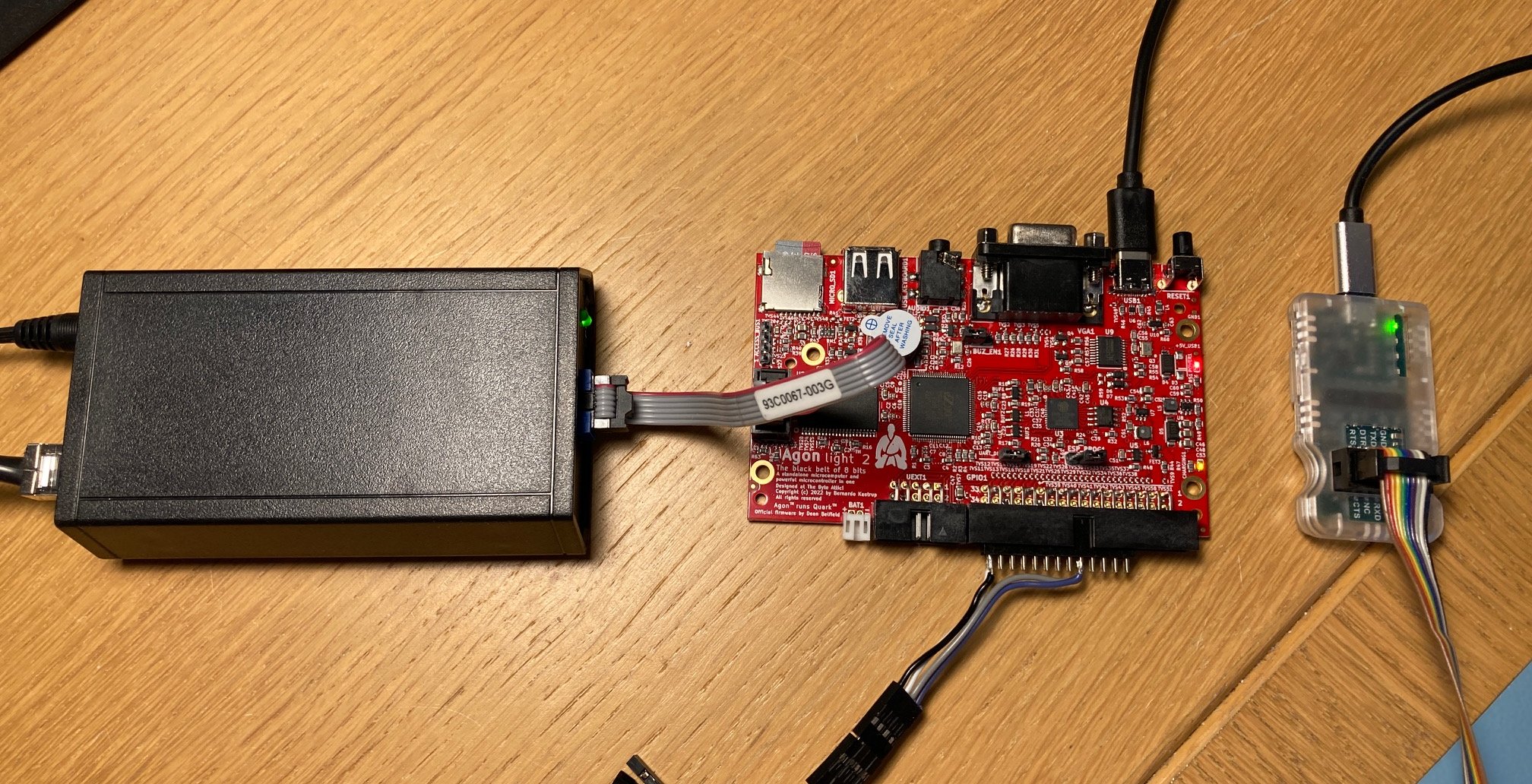
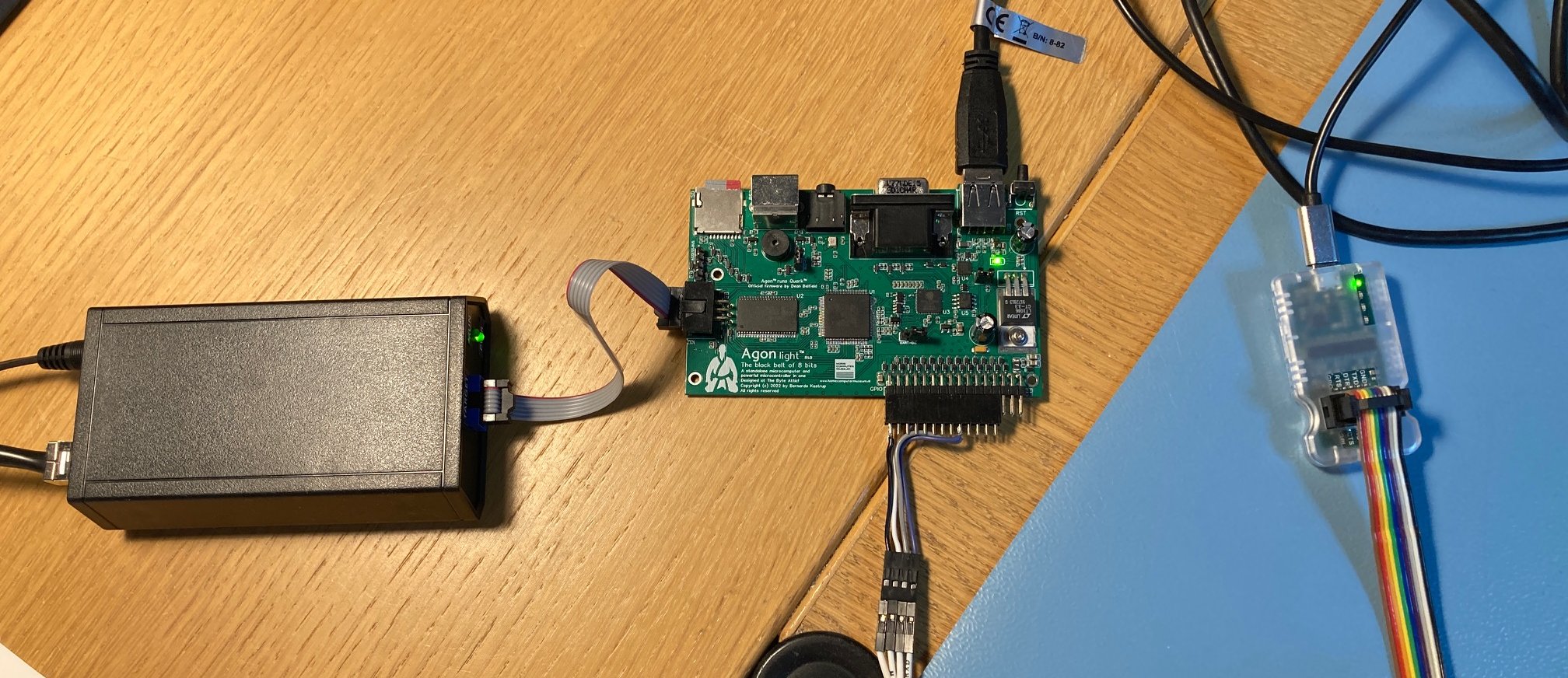
The Z20X PCB does not have a UART connector (I’m told this might change in the future however).
The pictures below show my current solution. I simply soldered a few wires on the expansion connector of the Z20X board knowing that the following pins are used for UART0:
Port D, bit 0 is TxDO (pin 68 on the eZ80F92, pin 57 on the expansion connector)
Port D, bit 1 is RxD0 (pin 69 on the eZ80F92, pin 58 on the expansion connector)


Power usage considerations
The Z20X computer is powered via a USB cable. However it does take quite some power when the SSD1963 display is installed as well (I measured up to 0.8A peak). You definitely need a powered USB hub if you intend to power the Z20X computer via a USB port. A better solution is to use a dedicated USB charger (at least 5 Watt).
Do I really have to do all this clicking and typing?
You can find a ready made Hello World project here.
Enjoy playing with your new toy :-)